In semiconductor manufacturing, the p-type silicon wafer and n-type silicon wafer are two fundamental materials that form the backbone of modern electronic devices. Both are derived from high-purity silicon, but they differ significantly in terms of doping elements, electrical behavior, charge carrier types, and application fields. These differences directly influence how chips, solar cells, and integrated circuits perform in real-world applications. Understanding the distinction between these two wafer types is essential for engineers, manufacturers, and anyone involved in the semiconductor or photovoltaic industries. The p-type silicon wafer in particular plays a crucial role in many traditional and cost-effective semiconductor designs due to its stable performance and mature production process.
Doping Elements and Material Composition Differences
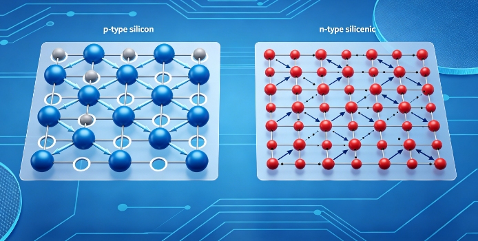
The primary difference between p-type and n-type wafers lies in the doping elements introduced into the silicon crystal structure.- P-type silicon wafer doping process: In p-type wafers, elements such as boron are added to pure silicon. These trivalent atoms create “holes” by accepting electrons, resulting in a positive charge carrier environment.
- N-type silicon wafer doping process: In contrast, n-type wafers are doped with phosphorus or arsenic, which have extra electrons, producing negative charge carriers.
- Atomic structure impact: The introduction of different dopants changes the crystal’s electrical behavior without altering its overall structural integrity.
- Electrical neutrality balance: Although both wafers remain electrically neutral overall, their internal charge movement mechanisms are fundamentally different.
Electrical Conductivity and Charge Carrier Behavior
One of the most important distinctions between these wafers is how they conduct electricity.- Hole-dominant conduction in p-type silicon wafer: Electrical current flows primarily through “holes,” which act as positive charge carriers moving through the silicon lattice.
- Electron-dominant conduction in n-type wafers: In n-type materials, electrons are the primary carriers, allowing faster mobility in many cases.
- Mobility differences: Electron mobility is generally higher than hole mobility, meaning n-type wafers can sometimes offer faster electrical response.
- Temperature sensitivity: P-type wafers often exhibit stable performance under varying temperature conditions, making them suitable for many standard applications.
Application Areas in Electronics and Solar Technology
Both wafer types are widely used, but their applications differ based on performance characteristics and cost considerations.- P-type silicon wafer in solar cells: Widely used in traditional photovoltaic panels due to lower production cost and mature manufacturing processes.
- Integrated circuit applications: P-type substrates are commonly used as base materials for CMOS technology in combination with n-type regions.
- N-type wafer in high-efficiency devices: N-type wafers are often used in advanced solar cells and high-performance electronics due to lower degradation rates.
- Industrial preference differences: Many mass-market semiconductor products still rely on p-type wafers because of their balance between cost and reliability.
Performance Stability, Efficiency, and Reliability Factors
When comparing performance, several technical factors distinguish the two wafer types.- Light-induced degradation resistance: N-type wafers generally perform better under long-term light exposure, especially in solar applications.
- Cost-performance balance of p-type silicon wafer: P-type wafers remain more cost-effective for large-scale production.
- Recombination rate differences: P-type materials tend to have higher carrier recombination rates compared to n-type wafers.
- Manufacturing maturity: P-type silicon wafer production processes are more established, ensuring consistent quality and lower production risk.
Manufacturing Complexity and Industry Adoption Trends
The production process and market adoption also highlight clear differences between these two wafer types.- P-type silicon wafer manufacturing efficiency: Easier and more cost-efficient to produce, making it widely adopted in global semiconductor supply chains.
- N-type wafer production complexity: Requires more precise control and higher purity levels during doping and processing.
- Market adoption trends: While n-type wafers are gaining popularity in high-efficiency applications, p-type wafers still dominate mainstream markets.
- Supply chain stability: Established infrastructure supports large-scale production of p-type wafers with consistent quality output.